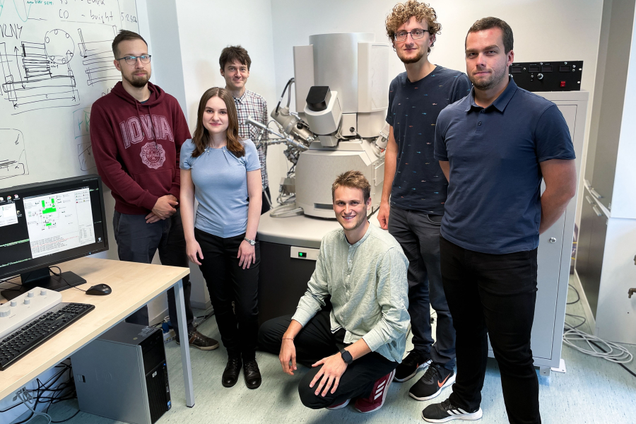
The Fabrication and Characterisation of Nanostructures research group conducts comprehensive research on nanostructures, from their design and fabrication to the detailed characterisation of their functional properties. We combine bottom-up methods, which rely on the self-organized growth of nanoobjects and ultrathin layers, with top-down techniques, particularly nanolithography, which enable the fabrication of structures with precision on the order of a few nanometers. This complementary approach allows us to produce nanostructures with precisely defined geometry and unique properties not found in conventional materials, spanning the fields of nanoelectronics, nanophotonics, plasmonics, spintronics, and (bio)sensing. An integral part of our work is also the utilization and development of our own analytical, microscopy, and metrology methods, which allow us to reliably characterise the properties of the fabricated nanostructures and provide a solid foundation for their further use in both science and practice.
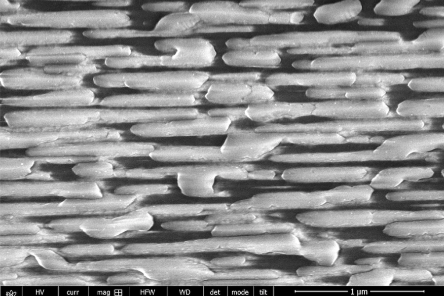
The results of our work extend beyond fundamental research and find concrete applications in key technological fields. Research on plasmonic nanostructures, including unique gallium nanoparticles, is paving the way for more sensitive sensors, advanced spectroscopic methods such as surface-enhanced Raman spectroscopy (SERS), and more efficient use of solar energy through broadband light absorption in solar cells. The study of magnetic nanostructures contributes to the development of spintronics and magnetic data storage, while the development of new materials, such as gallium nitride chips, has the potential to significantly reduce the energy demands of technologies used in telecommunications and e-mobility. Our long-term collaboration with leading industrial partners, particularly in the field of electron microscopy, further enables us to translate these findings directly into new technological and analytical devices – ranging from tools that allow chemical reactions to be carried out directly inside an electron microscope to methods offering significantly higher sensitivity in electron paramagnetic resonance. Through this connection between basic research and applications, our work actively contributes to technological progress as well as to addressing global challenges such as reducing CO2 emissions.
Over the course of its existence, our group has achieved a number of significant results with international impact. As part of the European ALL2GaN project, we collaborate on the development of materials for energy-efficient gallium nitride chips, while the international PETER project has produced a new, significantly more sensitive electron paramagnetic resonance method capable of analyzing materials down to the microscopic level. In the field of electron energy loss spectroscopy, we were the first in the world to explore the limits of the Babinet principle for plasmonics and to map plasmon resonances in plasmonic nanoantennas, research we are now extending to the interaction between antennas and apertures. We have also contributed to international research on the unique material VO2 for the fabrication of large-scale metasurfaces, in collaboration with teams from the USA and Hong Kong. Our ability to translate scientific findings into practice is demonstrated by NenoVision, CEITEC BUT's first-ever spin-off company, born from research into the integration of atomic force microscopy and electron microscopy, which is now followed by a new Technology Agency of the Czech Republic project focused on the further development of the LiteScope microscope in collaboration with other academic institutions. Recognition for our approach also came in the form of a win in the Technology Agency of the Czech Republic competition with a prototype electron microscope enhanced with an atomic source enabling chemical reactions to be carried out directly during sample observation.