
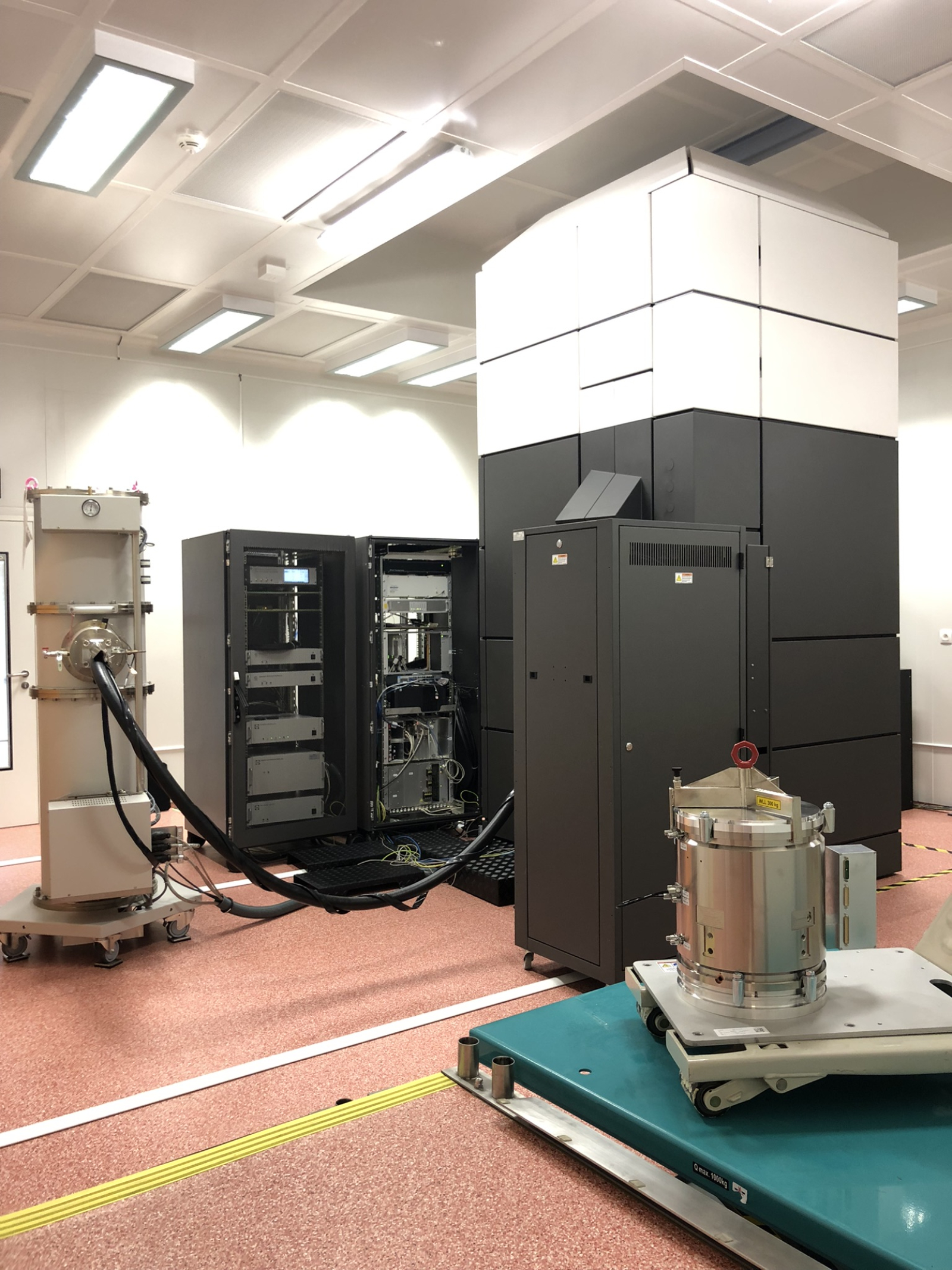
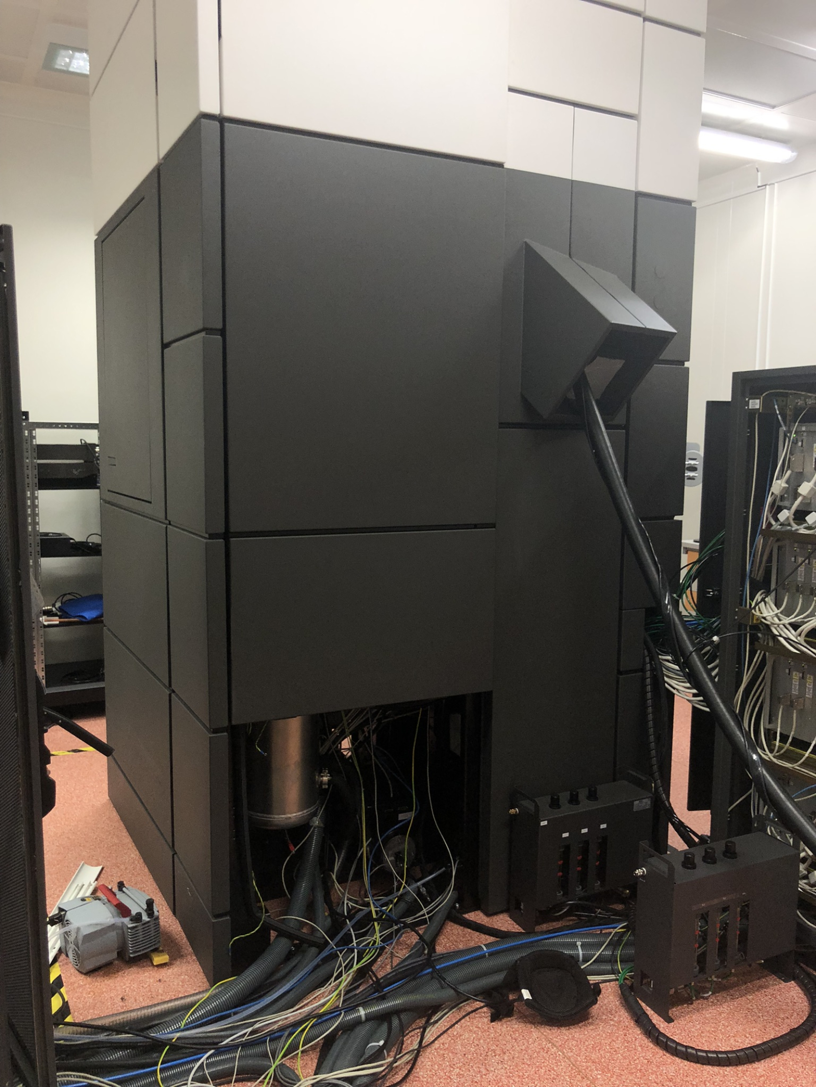
The clean laboratories of the CEITEC Nano research infrastructure at CEITEC Brno University of Technology house a TITAN transmission electron microscope, approximately four meters high, for research into materials at the atomic level. This scientific device underwent two significant upgrades last year, entailing the addition of two state-of-the-art technologies: an electromagnetic lens aberration corrector for scanning transmission electron microscopy and an electron energy loss spectrometer equipped with cameras featuring today's most sensitive sensors. Thanks to these modernization steps, TITAN has become a state-of-the-art device that can only be found in a few of the world's most advanced laboratories in this configuration.
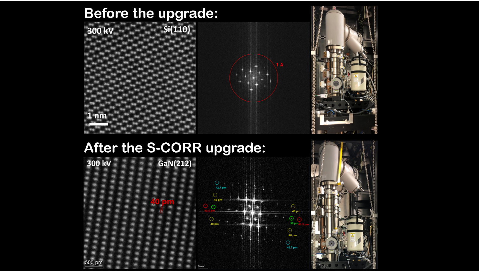
The TITAN Themis transmission electron microscope (TEM) was manufactured in 2015 by FEI (now Thermo Fisher Scientific, US) and has been used for research purposes at CEITEC BUT since 2016, employing a range of imaging and analytical microscopy techniques. At that time, it was already one of the most powerful commercially available electron microscopes in the world, but it did not have a corrector for aberrations (i.e., imperfections) in the lenses forming the narrow electron beam scanning the sample. This meant that the microscope took images with lower resolution, and it was difficult or impossible to analyze the chemical composition or physical properties of samples at the atomic level. “The latest generation S-CORR aberration corrector allows a narrower electron beam interacting with the sample to be focused to a size up to twice smaller than an atom, while also providing a higher electron current. This has resulted in a significant increase in the maximum resolution when taking images and also improved its analytical capabilities at the atomic level. Thanks to the new corrector, which we financed through the JAK CzechNanoLab+ operational program, our microscope achieves the world's highest standard in resolution, specifically less than 50 pm at the highest electron acceleration voltage of 300 keV,” says Jan Michalička, guarantor of the TITAN microscope. “To illustrate the dimensions we are dealing with, imagine the ratio of the size of a golf ball to that of our Earth. And that is precisely the ratio of an atom with size of 100 pm to a golf ball.” He adds that thanks to this resolution and beam intensity, scientists are now able to recognize individual atoms distributed on the surface of atoms of another material and use spectrometry to measure what kind of atoms they are. This is a crucial capability, for example, for the development of more efficient single-atom catalysts in hydrogen production.
The installation of a corrector with state-of-the-art design of its electron optics also brings the important ability to image and analyze materials at atomic resolution using electrons accelerated in the microscope at low energies. Electrons passing through the sample interact strongly with it, which means they can damage it at the atomic level. The material can thus evaporate locally or change its structure and chemical composition, and in subsequent analyses, scientists are already looking at the altered state of the specimen. Examples of such sensitive materials include graphene and other intensively studied atomic monolayer materials, which can be analyzed without damage only by electrons accelerated to sufficiently low kinetic energy. “With the new corrector, we can examine samples with atomic resolution below 100 pm even at the lowest acceleration voltage of the microscope, 60 keV. Ultimately, this allows us to study even the most sensitive materials in a virtually unchanged state, which is exactly what we need for our work. TITAN can now observe, for example, defects in the arrangement of carbon atoms in graphene without inducing further defects with its electron beam.”
The additional installation of a corrector in the CEITEC laboratory is unique in the world
The corrector of optical aberrations in electromagnetic lenses is an exceptional technology that has completely changed the world of electron microscopy. It could be said that it should never have been created because in the scientific world, correcting defects in electromagnetic lenses was considered impossible. The spherical aberration that these correctors primarily eliminate can theoretically be eliminated with a concave lens. This is common in light optics, but it cannot be manufactured as an electromagnetic lens. Alternative designs for optical systems, i.e., the first correctors, were technically too complex to manufacture at the time, and their adjustment was limited by the computing technology available at the time. The lack of correctors thus essentially limited research into the structure and properties of materials at the atomic level. In the 1990s, however, a group of four scientists, Harald Rose, Max Haider, Knut Urban, and last but not least Ondřej Křivánek, originally from Czechia, succeeded in creating correctors based on the principle of multi-magnets. “Correctors basically consist of a pair of complex lenses, each containing a series of magnetic multipoles. In the case of the correctors invented by the first three scientists, spherical aberration is eliminated by two hexapole lenses. Our new corrector also uses this concept. The corrector invented by Ondřej Křivánek and his team in the USA uses a quadrupole-octupole lens system,” explains Jan Michalička. All of the scientists mentioned above received the prestigious Kavli Prize in the nanoscience category in 2020 for their discovery, specifically for significant innovations in atomic resolution electron microscopy.
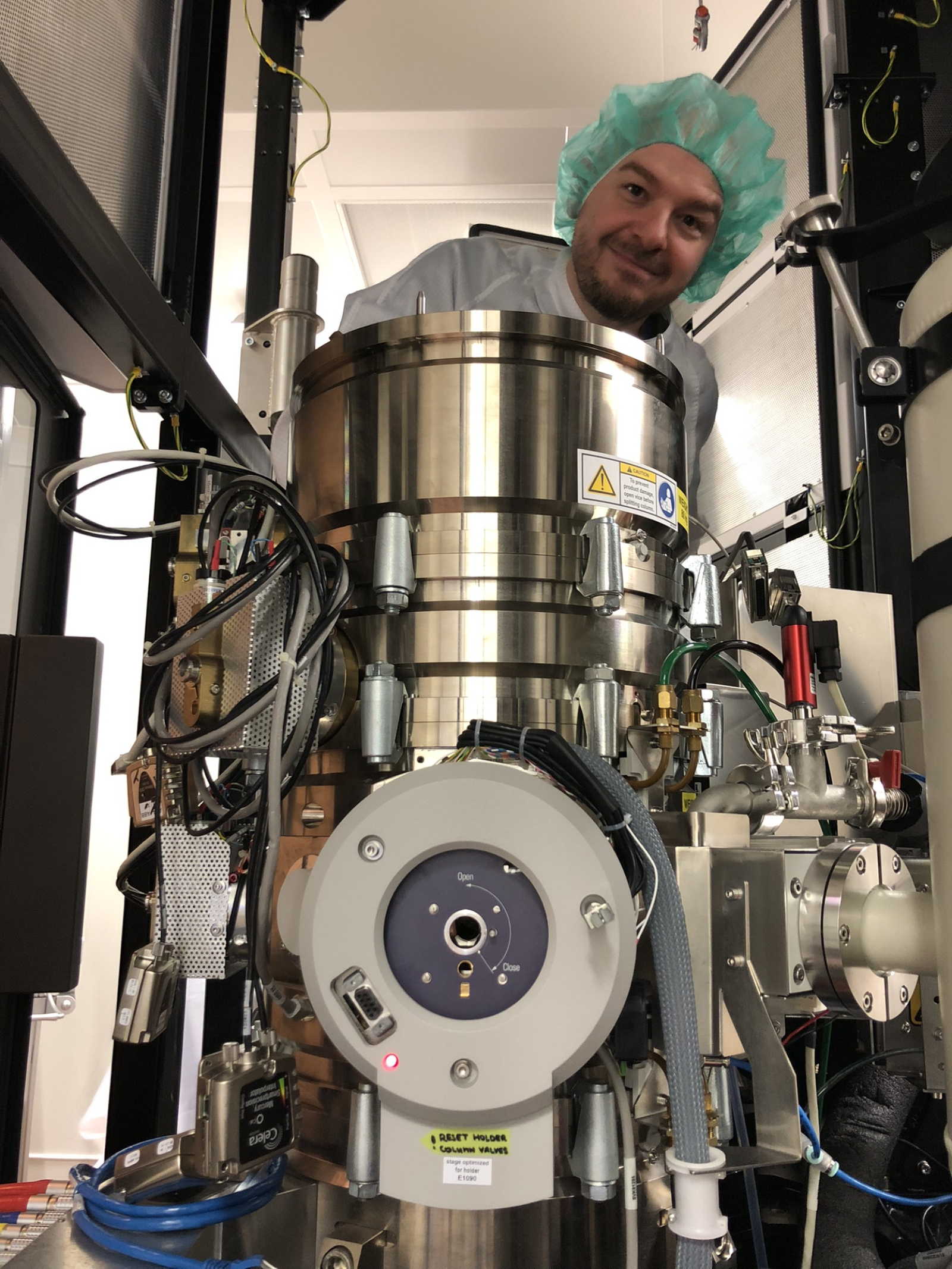
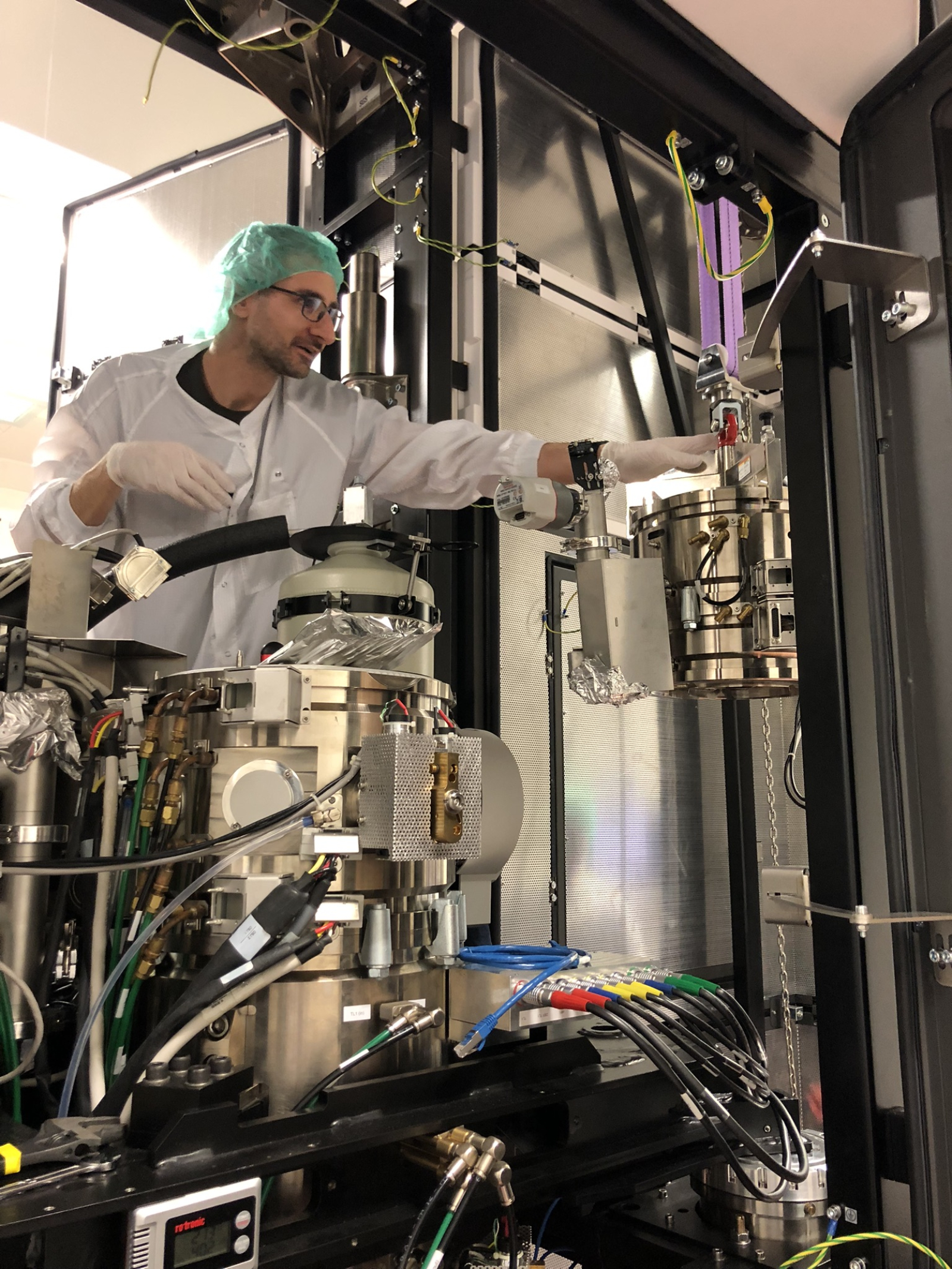
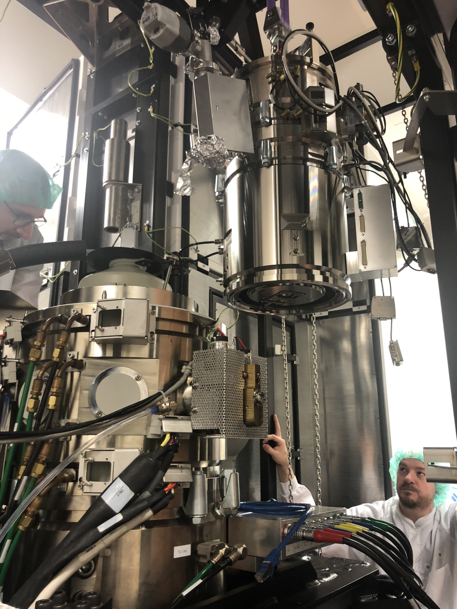
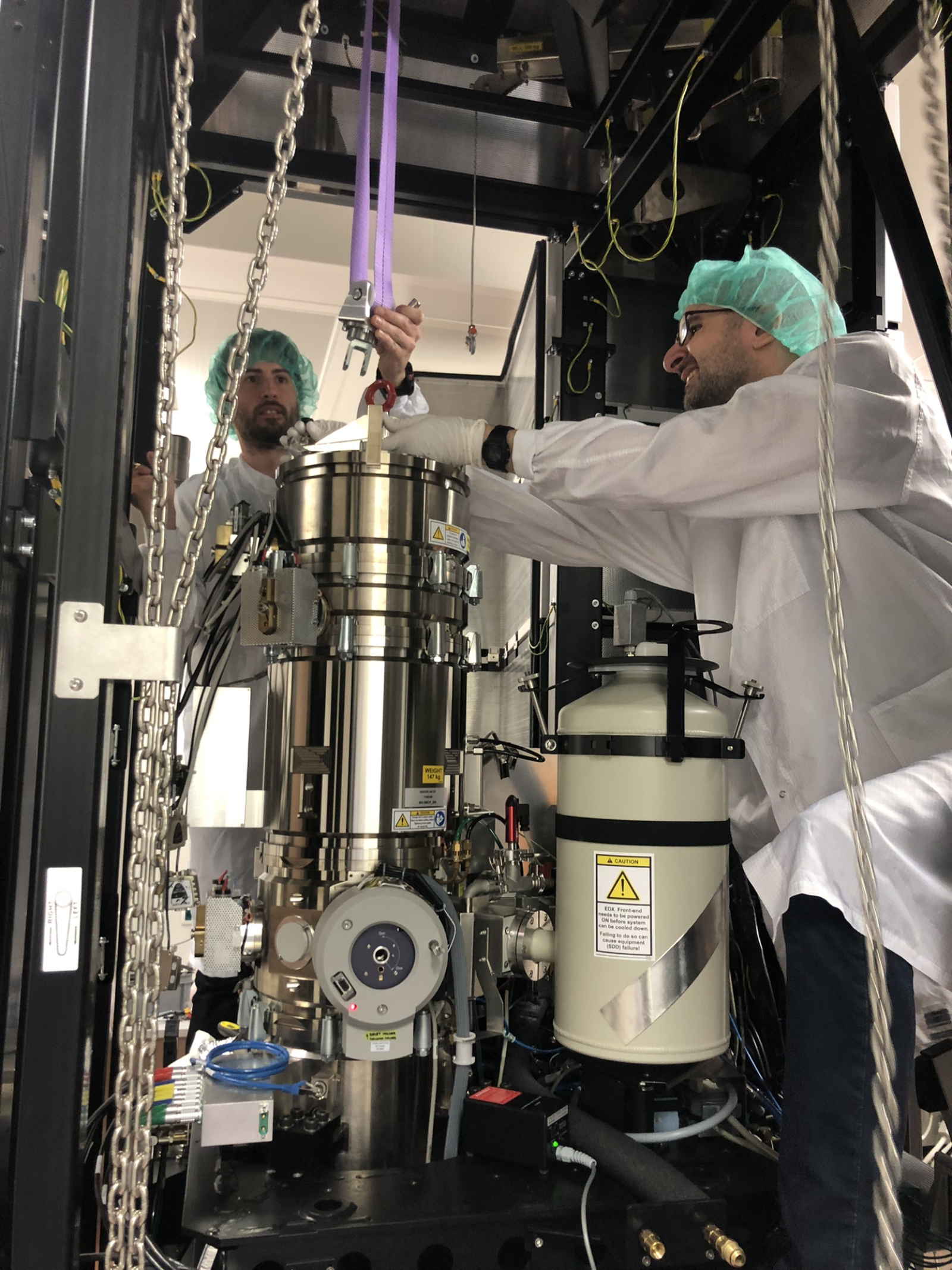
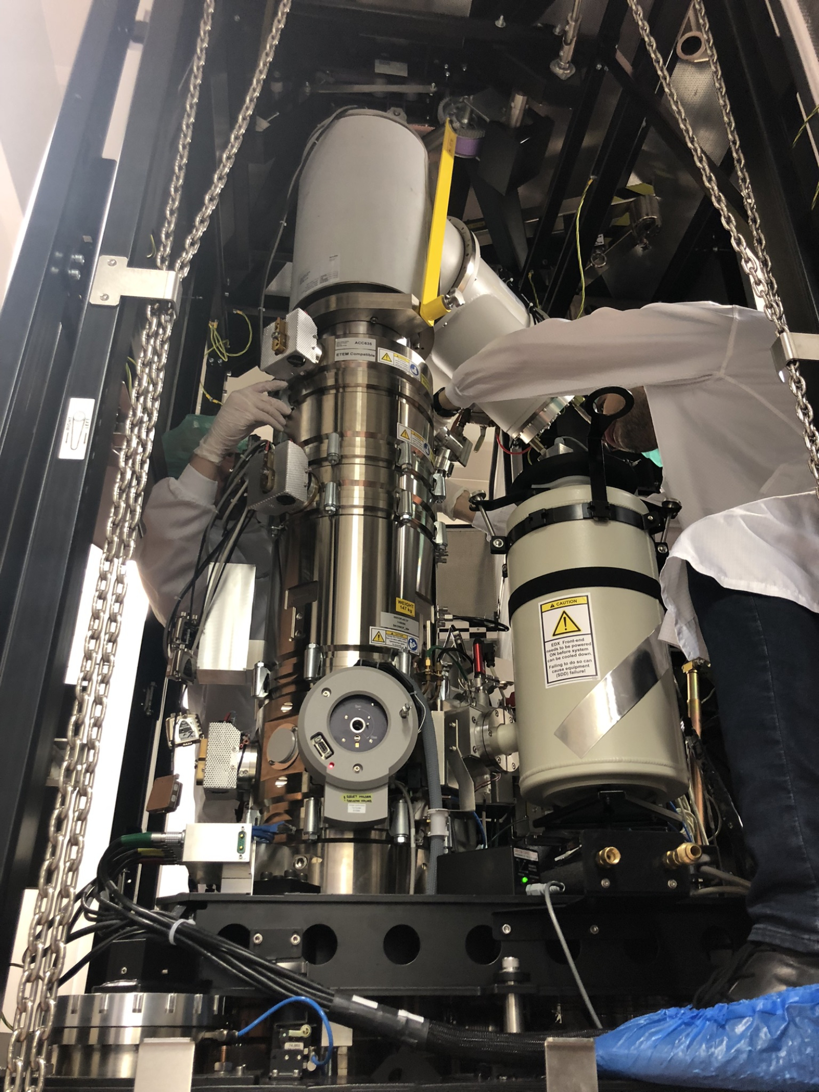
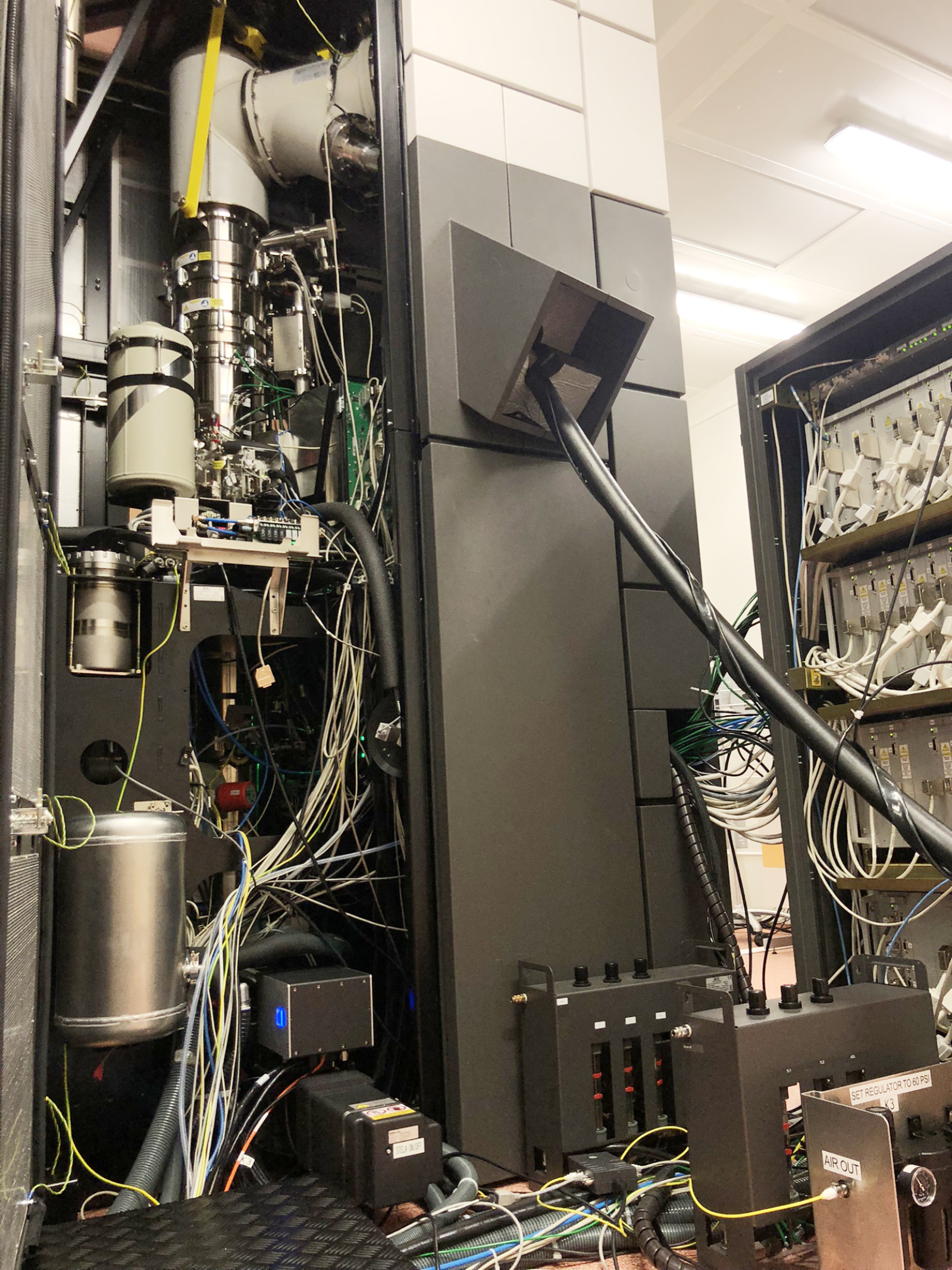
But back to the TITAN microscope. It is located in a dedicated cleanroom laboratory, where it is housed within a massive steel enclosure mounted on a 1.5-meter-deep isolated concrete block to ensure complete isolation from acoustic and structure-borne vibrations. The entire laboratory is also equipped with an active compensation system that suppresses external electromagnetic interference originating from surrounding equipment and technologies within the institute’s premises. TITAN not only has atomic resolution, but also high sensitivity to all of these types of interference. In addition to the microscope itself, the laboratory also houses its complete control and computing infrastructure and other technology necessary for its operation. The installation of the corrector took about three months on site and required the dismantling of almost the entire microscope, followed by lengthy fine-tuning to achieve the correct parameters. “Since the entire device is a vacuum system, it was necessary to ensure that all parts were assembled with precision so that there were no gaps through which air could flow into the microscope tube. At the same time, the microscope is composed of a whole series of sub-systems that must finally work together perfectly, so getting the microscope up and running was an engineering challenge,” notes Jan Michalička.
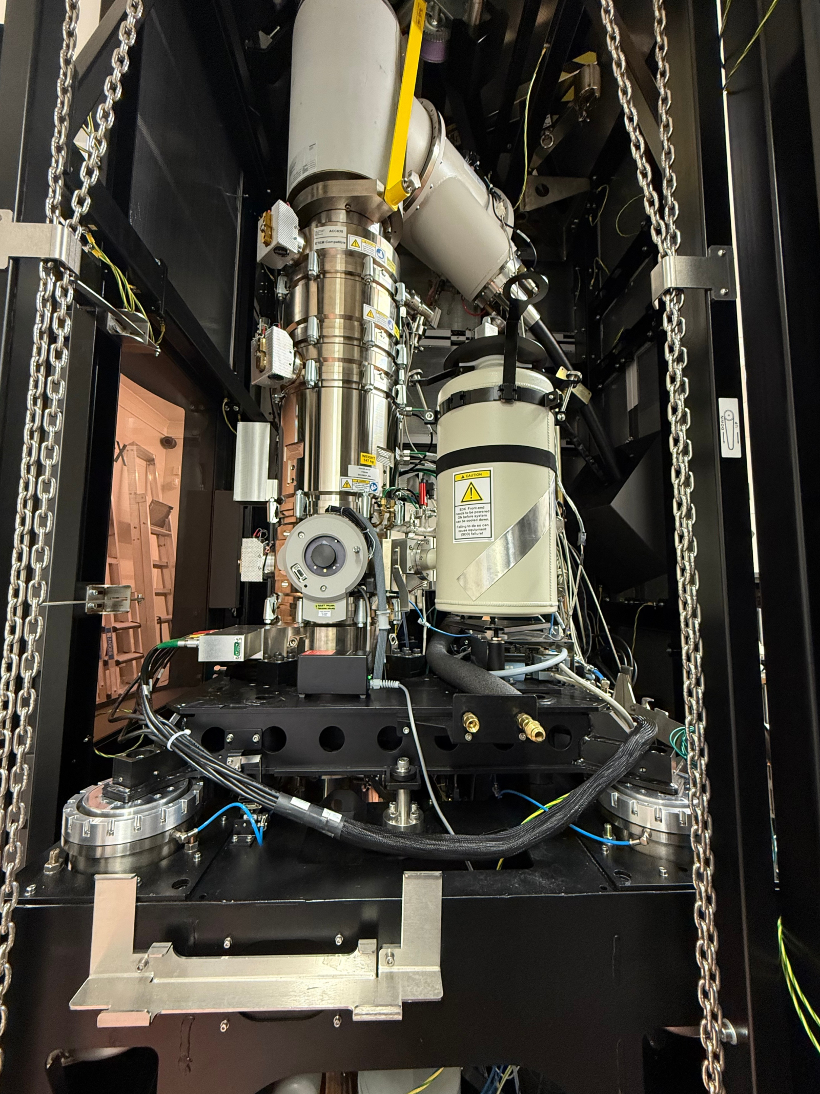
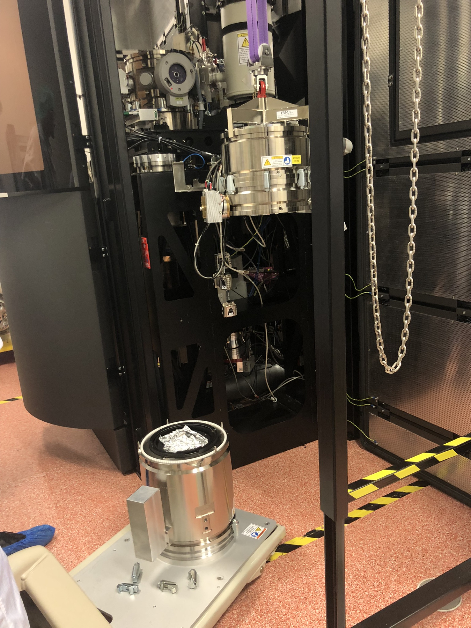
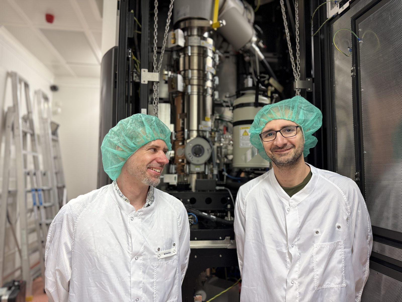
The corrector itself weighs 147 kg and is located between the condenser and objective lens. “Our project to retrofit older equipment with a corrector is truly unique in the world, because correctors are normally installed directly at the microscope manufacturer's factory. We basically went back to the time when the four scientists mentioned above placed their prototype corrector on an older microscope and improved its performance,” says Jan Michalička with a smile, adding that the most difficult part of the entire microscope modernization was adjusting the corrector and the entire microscope optics, which took two months. “Even though most things are now controlled by computers, there are only a few people in the world who can install and tune the corrector to the highest level of accuracy, and in our case at three different voltages: 60 kV, 120 kV, and 300 kV. We are therefore extremely pleased that we had two of these experts available here at CEITEC.”
New spectrometer will make it possible for scientists to see more
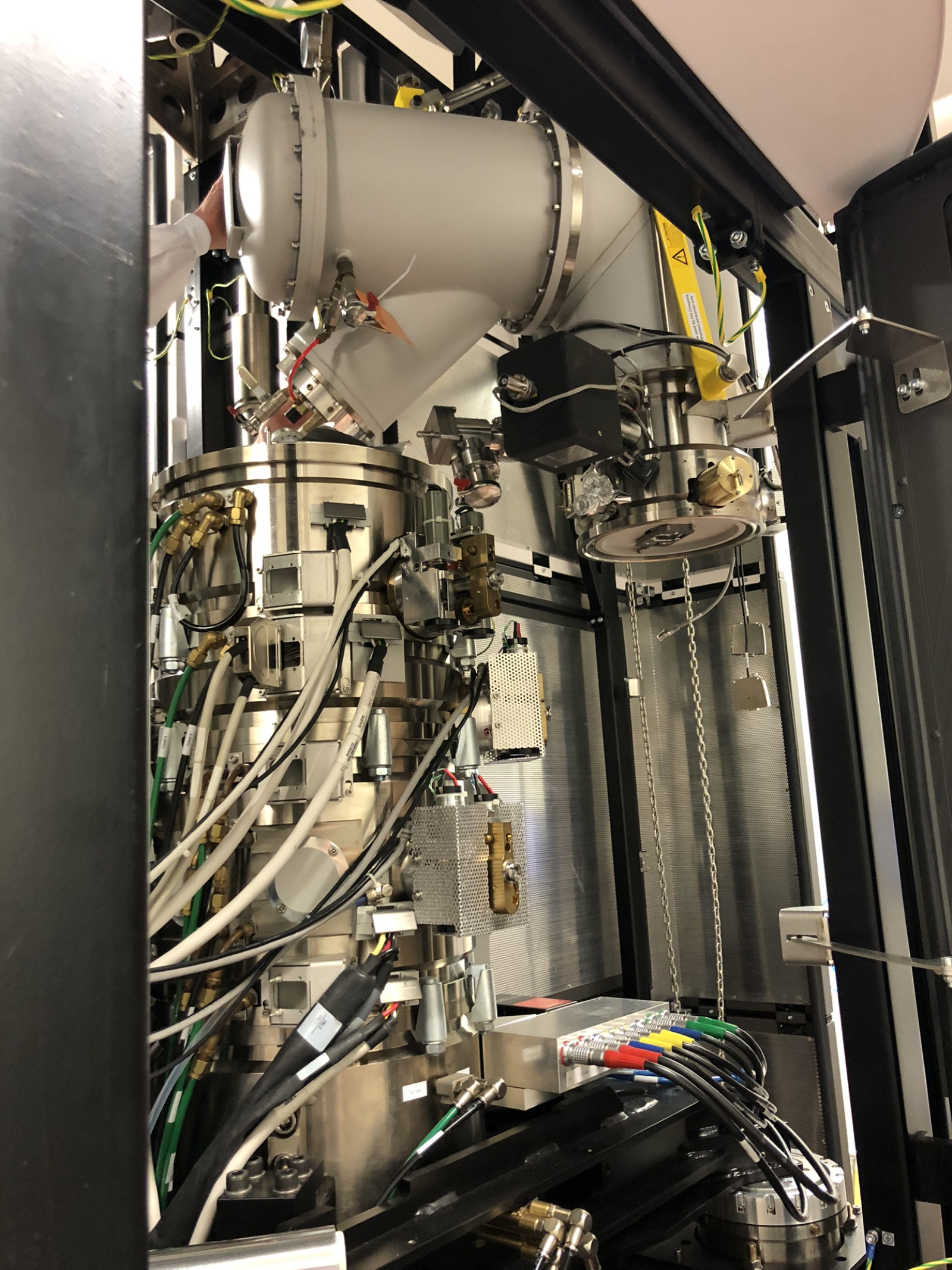
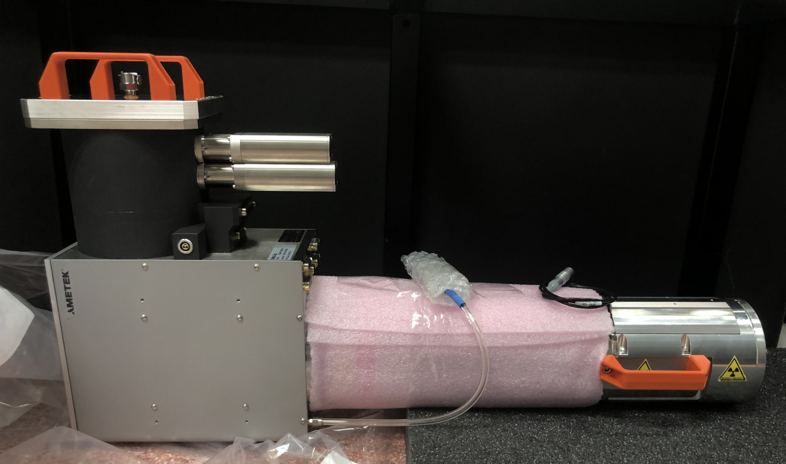
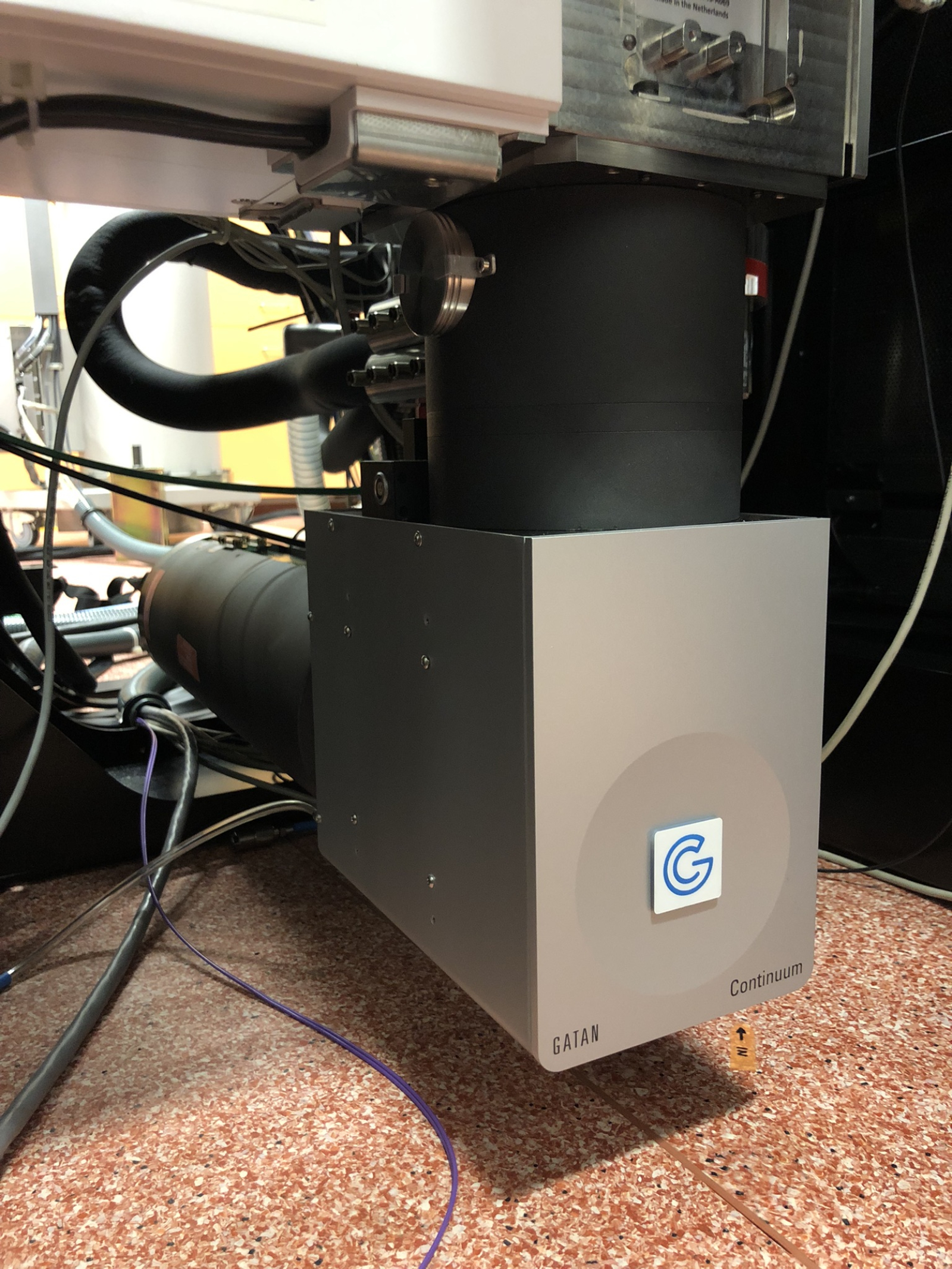
However, the TITAN microscope boasts more than just the new aberration corrector. The second, equally important upgrade is the installation of the latest generation of the GIF Continuum HR electron energy loss spectrometer by Gatan (US). It is an approximately two-meter-long device installed horizontally under the entire microscope, as its main component is a magnetic prism that disperses the electron beam according to the energy losses of electrons that occurred when the beam transmitted through the sample. The resulting beam then passes through the complex electron optics of the spectrometer, similar to the one in a corrector, which in this case precisely focuses the electron beam onto a camera in the form of a spectrum showing intensities of these energy losses (EELS mode), or, in the form of an image formed by electrons with a certain energy loss (EFTEM mode). Electron energy losses are extremely informative about the sample, principally at the atomic level, as they are characteristic of the given state of the atoms, such as the valence arrangement of their electron shell. In this way, it is possible to precisely analyze the chemical bonds between atoms, the structural arrangement of atoms in a crystal lattice, or a variety of physical properties of nanostructures. In combination with the new corrector, that allows the sample to be scanned with an atomically narrow beam, this information can be obtained literally from individual atoms.
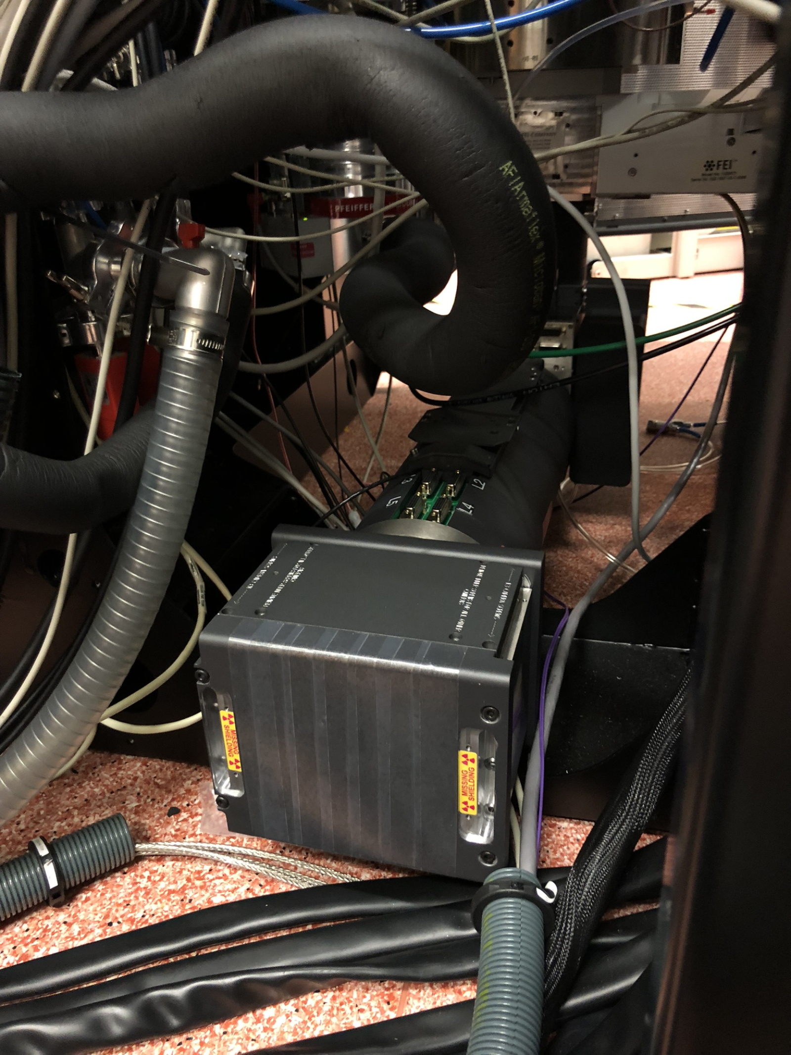
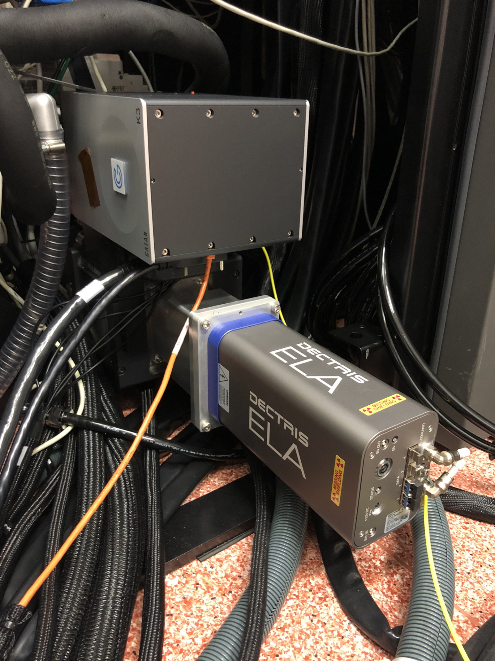
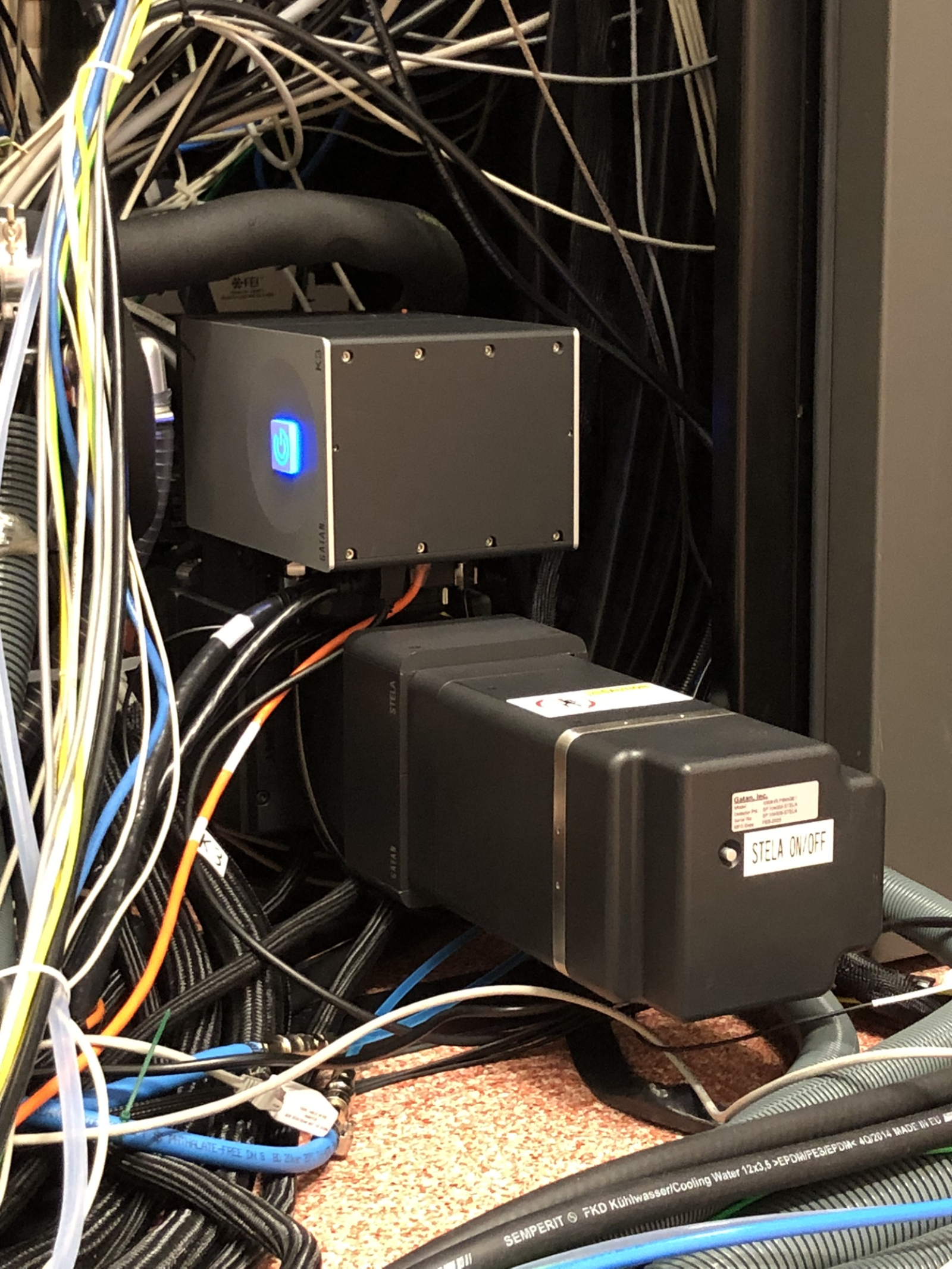
A key component of the new spectrometer is the state-of-the-art K3 and Stela cameras, whose sensors enable the direct detection and counting of individual electrons incident on them. This gives them unprecedented detection sensitivity and almost no noise in data compared to cameras of older generations. At the same time, these cameras are extremely fast – for example, the Stela camera can record up to 16,000 spectral images per second. Thanks to these features, the data can be collected from a defined area of specimen much faster and thus with much lower electron dose. This is again crucial for all samples sensitive to electron damage or for dynamic experiments in which changes occur in the sample, even at the atomic level. In addition, thanks to its advanced cameras, the new spectrometer can compete with scientific equipment such as synchrotrons. “When we used older cameras, we couldn't detect high-energy spectral K-edges of heavier elements because they were noisy due to the weak signal. But the higher sensitivity of the cameras will allow us to obtain these very important results for the first time, which normally require the use of a synchrotron and X-rays (XAS technique). However, unlike the XAS technique, which has a maximum spatial resolution in the order of tens of nanometers, our upgraded microscope will enable this up to the atomic level, which is an unprecedented qualitative advancement in this field of microscopy,” notes Jan Michalička.
Last but not least, the spectrometer will open up completely new possibilities for measuring the magnetic properties of atomic structures using techniques such as magnetic circular dichroism of electrons or differential phase contrast imaging, for which it is fully equipped. The new spectrometer will be used for experiments within the Jan Ámos Komenský TERAFIT operational program, which funded the upgrade at CEITEC. This program focuses on research into spintronics and the magnetism of materials for ultra-high capacity, speed, and energy efficiency in information technology. “At the same time, it has advanced algorithms for automatic calibration and correction and offers integration with advanced artificial intelligence and machine learning software for data visualization and evaluation,” adds Vojtěch Uhlíř, head of the Nanomagnetism and Spintronics research group at CEITEC BUT and one of the TERAFIT project investigators, listing the spectrometer’s other advantages.
Together with the corrector, the spectrometer is a game changer in the field of material property analysis. According to Jan Michalička, CEITEC now has one of the most powerful microscopes: “In modern materials science, for example in the development of magnetic memories, quantum materials, or 2D structures, it is necessary to see not only atoms, but also their behavior in real time, including magnetic states. And it is precisely this spectrometer that pushes the boundaries of what we can see and analyze.” Michal Urbánek, head of the CEITEC Nano laboratories and coordinator of the large research infrastructure CzechNanoLab, agrees with him, adding that the device can now contribute to scientific knowledge on a global scale. “Thanks to its integration into the large CzechNanoLab research infrastructure, this state-of-the-art microscope is accessible not only to scientists from CEITEC, but also to other institutions in the Czech Republic and abroad."
Photogallery
Expert
