
24. Apr. 2026
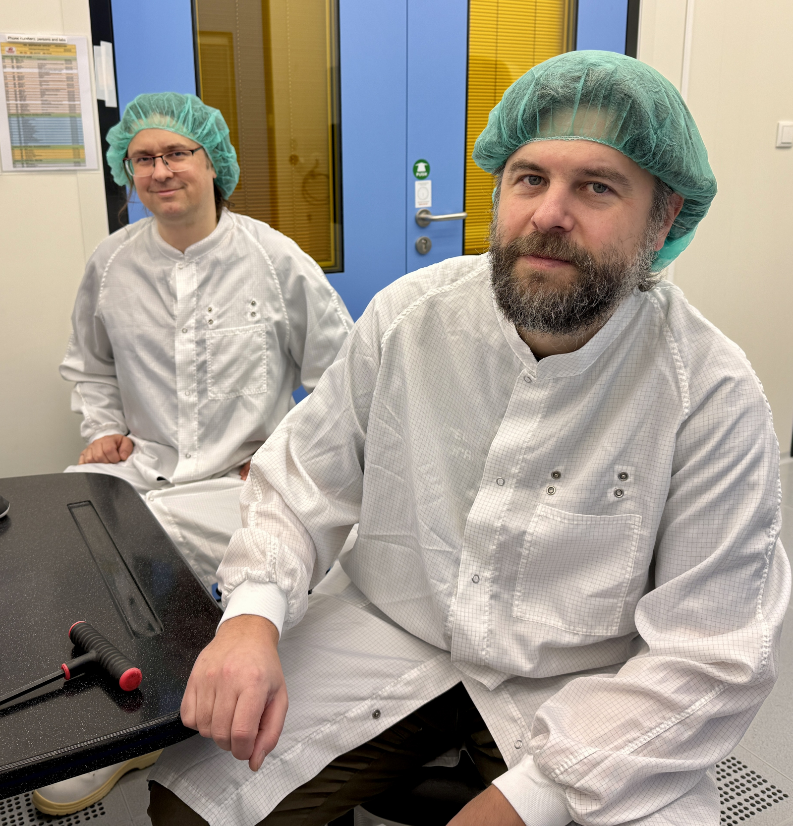
In February of this year, a GAČR project focused on high-speed scanning probe microscopy was launched. Over the next three years, scientists from CEITEC Brno University of Technology (BUT), in collaboration with the Czech Metrology Institute (CMI), will work to accelerate measurement processes using this technique and to improve the analysis of the acquired data with the help of custom-developed artificial intelligence algorithms. The research results will find applications in both scientific and industrial practice, for example, in monitoring live cells or in chip manufacturing.
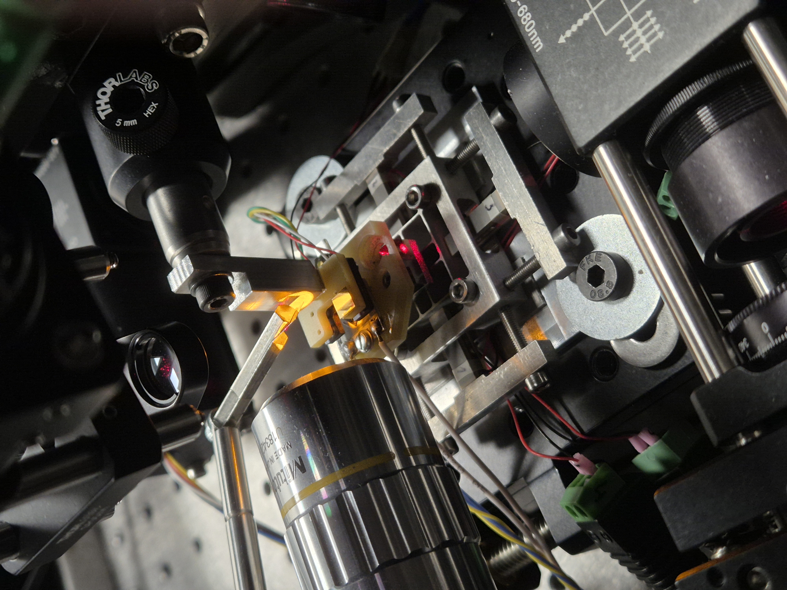
High-speed atomic force microscopy is a field that allows scientists to study the properties of surfaces of various materials. They use microscopes equipped with a miniature tip and probe only a few nanometers (a millionth of a millimeter) in size, which repeatedly glide along regular paths across the sample surface. The scanned area is on the order of micrometers – smaller than a human red blood cell – and the surface shape is recorded with precision comparable to the distance between individual atoms. The probe scans the surface, enabling scientists to obtain highly detailed images with extremely high resolution. Such measurements usually take only a few minutes, but even that can be too long in some cases, especially for samples that change over time, such as living biological materials, as well as non-living materials whose changes are of interest. Addressing this challenge is the core of the GAČR project, officially titled High-Speed Atomic Force Microscopy with Sparse Sampling.
“Our joint work aims to speed up the scanning process by optimizing the path along which the microscope tip moves, so that only truly useful data is measured. At the same time, we want to develop an algorithm capable of evaluating images without the need for an intermediate step of reconstructing data from the omitted parts of the surface,” says principal investigator Petr Klapetek from the Czech Metrology Institute (CMI). He points out that conventional high-speed scanning produces hundreds of images across the entire surface, but for samples that change rapidly over time, the probe may miss the area of interest at a critical moment. Changes occurring within milliseconds may therefore not be captured continuously, and important details can be lost. Researchers worldwide have been seeking ways to speed up scanning, usually by modifying microscopes so that the tip moves faster. However, mechanical acceleration increases error rates, for example, due to excessive vibrations. “Since we are aware of the inherent limits of scanning microscopy, we decided to take a completely different approach and tackle the problem through smarter measurement rather than major hardware modifications,” Petr adds.
Software-based acceleration to overcome design limits
One of the main tasks of the project will therefore be to design new scanning paths. These will remain regular but will be arranged in entirely different patterns to maximize the amount of information obtained in minimal time. Combined with more efficient data processing, this approach could increase scanning speed by up to five times. “Data processing is absolutely crucial for us. We need to develop AI algorithms capable of analyzing and interpreting images directly from such sparsely sampled grids, without needing to know what happened in the unmeasured areas. That will likely be our biggest challenge,” adds co-investigator David Nečas from CEITEC BUT. CEITEC BUT will be responsible for designing the scanning patterns and developing the necessary mathematical methods, while the experimental part – including all measurements and testing – will take place at the CMI.
The outcome of this three-year collaboration should be a comprehensive theoretical methodology supported by experimental procedures. It could be used, for example, in biological laboratories studying changes in the behaviour of living samples – typically cells – over time. It may also find applications in semiconductor labs, where high-speed scanning microscopy is used mainly for quality control and defect detection during chip production. The method can measure not only the shape and surface structure of a sample, but also its electrical and other properties. “In practice, it could eventually become part of specialized industrial applications, where high-speed scanning microscopes perform imaging and evaluation almost in real time within inspection lines,” concludes David Nečas.
Brno University of Technology is also currently collaborating with the Czech Metrology Institute and other academic and industrial partners on the European project DINAMO, which focuses on developing data-processing methods for calibrating all types of scanning probe microscopes. The team at BUT, led by principal investigator David Nečas, is working on standardizing these methods so that even scientists who are not specialists in this type of microscopy can easily set up the instruments themselves and measure their samples as accurately as possible.
Author: Kristina Blűmelová
Photogallery
Expert
