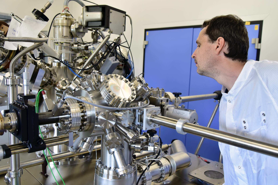
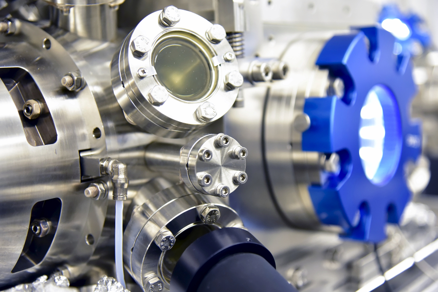
We investigate the phenomena essential for the growth of ultrathin layers, 2D materials, and self-organized nanoobjects with specific properties, such as nanowires, nanotubes, and quantum dots. We use physical vapor deposition (PVD) methods, including molecular beam epitaxy (MBE) and magnetron sputtering, as well as chemical vapor deposition (CVD, PECVD) and electrochemical methods. We pay particular attention to the initial stages of growth, which critically influence the properties of the resulting nanostructures – including substrate effects, nucleation and diffusion of atoms, and layer growth modes. We also work on the fabrication of semiconductor nanowires using the vapour-liquid-solid (VLS) method and monitor their growth in situ using electron microscopy.
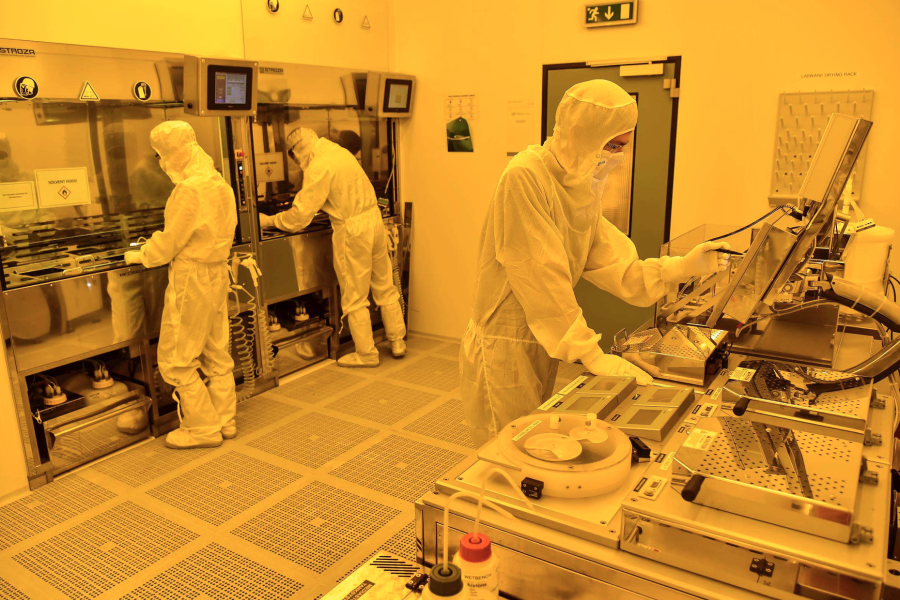
We develop nanolithographic methods based on electron beams, scanning probe microscopy (such as local anodic oxidation), or focused ion beams, allowing us to create nanostructures with minimum dimensions of around 10 nm. We focus on fabricating nanodevices such as quantum point contacts, single-electron transistors, and spintronic systems, on preparing ordered metallic nanoparticles for plasmonics, on dielectric and semiconductor nanocrystals for photonics, and on metallic and graphene nanoelectrodes for contacting molecular and magnetic nanostructures. An important part of our work is also the selective and controlled growth of nanostructures on substrates patterned by lithographic methods.
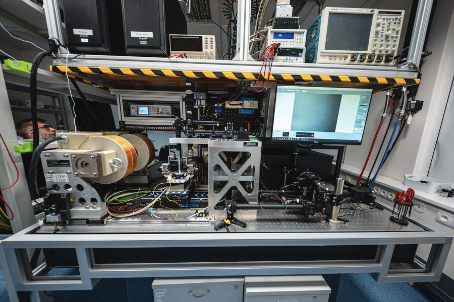
Our goal is to identify the relationship between the properties of nanostructures and their geometric and structural parameters. We study metallic nanostructures suitable for plasmonics, particularly the generation and detection of surface plasmon polaritons and their use in surface-enhanced Raman spectroscopy (SERS) and biosensing. We investigate magnetic 2D–0D nanostructures and their magnetic anisotropy, transport properties (GMR, TMR), and domain wall dynamics for spintronics and magnetic data storage. We also study the electronic structure and transport properties of graphene and other 2D materials, including the effects of adsorbates and radiation on their behavior.
We develop methods and methodologies for the microscopy, analysis, and metrology of nanomaterials, enabling precise diagnostics of their properties. We combine techniques such as scanning probe and electron microscopy, focused ion beam, optical methods, Auger electron spectroscopy, and electron paramagnetic resonance. We use these advanced methods not only in our own research but also for the characterization of nano- and microstructures in general, contributing to the development of the entire field of nanometrology.